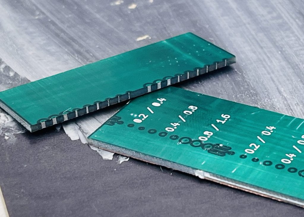
We have been testing in-house PCB processing methods and wanted to evaluate a very simple conductive epoxy fill method for make connections on either side of a two-layer printed circuit board (PCB).
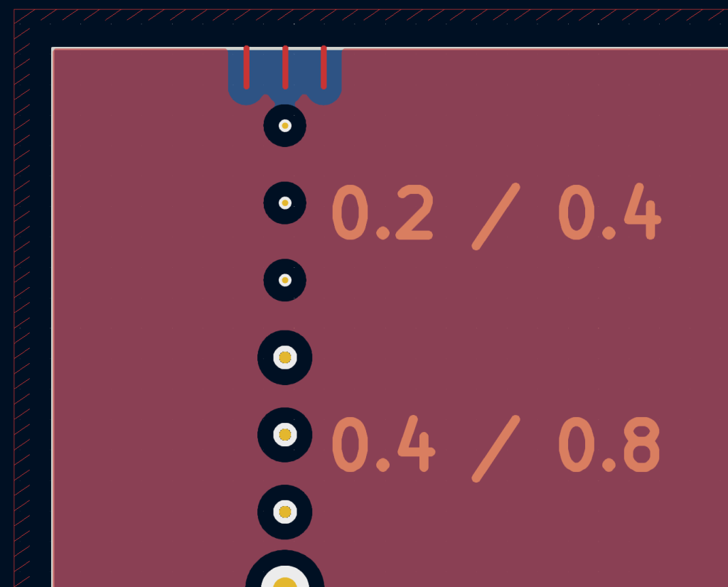
Our basic approach was to create a PCB with 3 via sizes:
- Via hole: 0.2mm / Via diameter: 0.4mm
- Via hole: 0.4mm / Via diameter: 0.8mm
- Via hole: 0.8mm / Via diameter: 1.6mm
The PCB design was achieved using an IR laser on standard 1.62mm FR4 with 1oz copper. Conductive epoxy (MG Chemicals 8331-14G) was spread along the etched copper on one side and a squeegee was used to push the epoxy into the vias. The epoxy was left to set for >24 hours before processing the solder mask and paste.
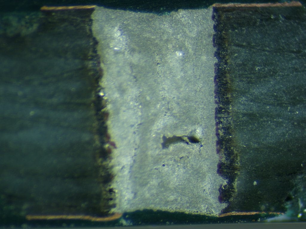
Visual Inspection
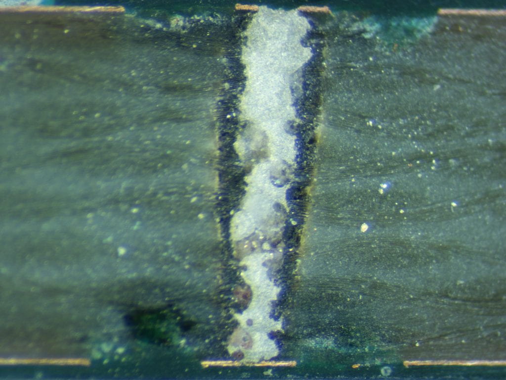
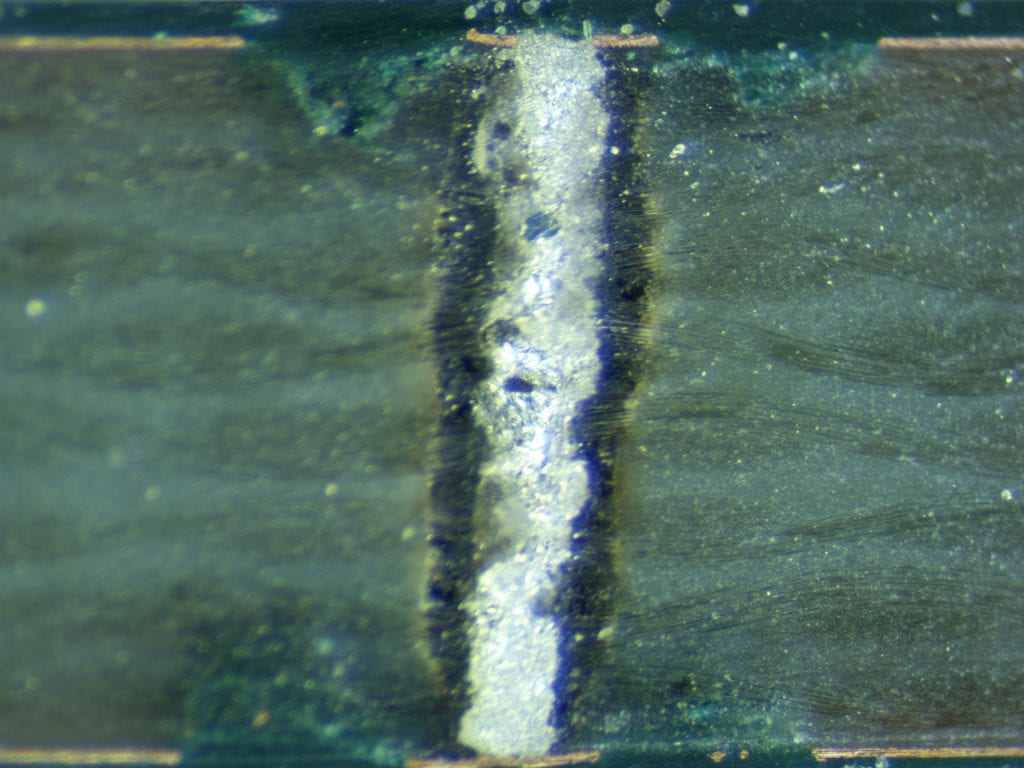
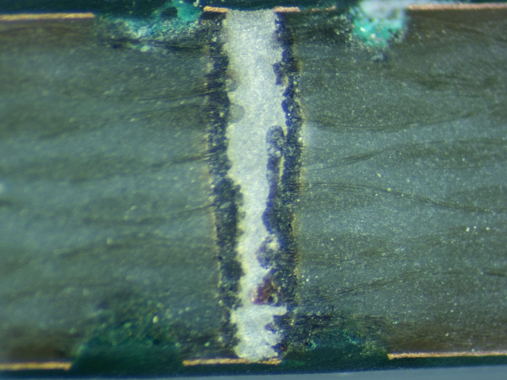
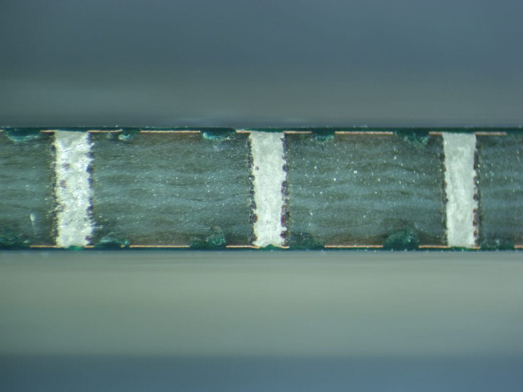
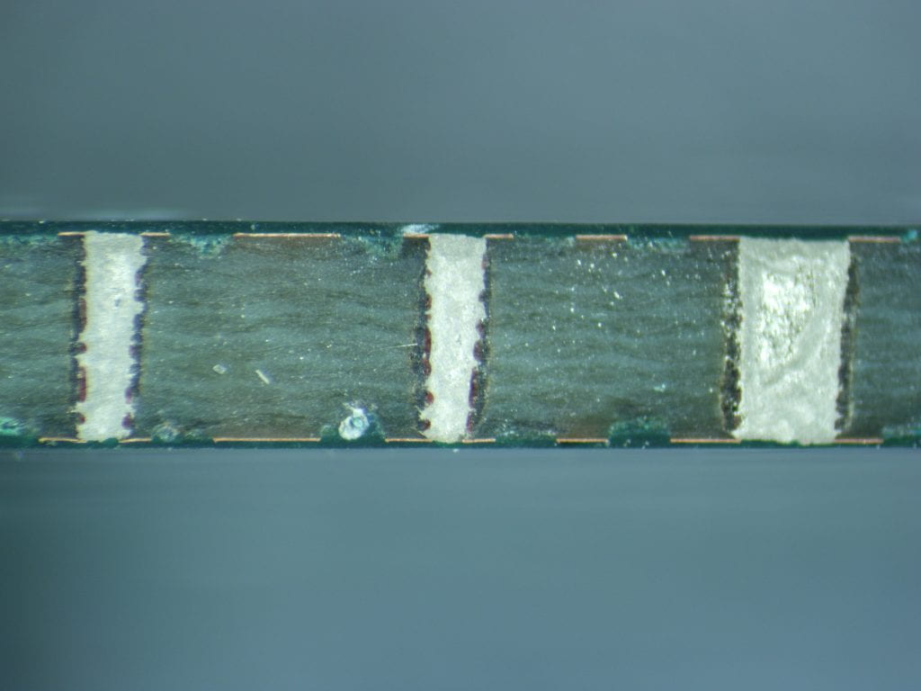
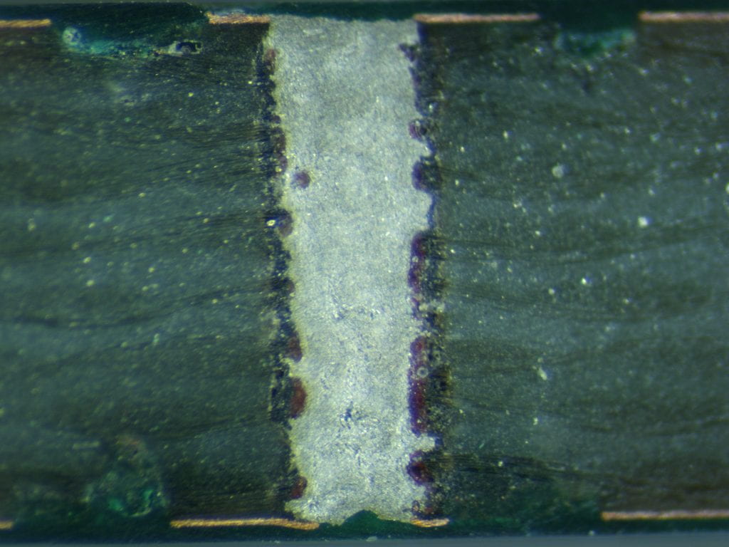
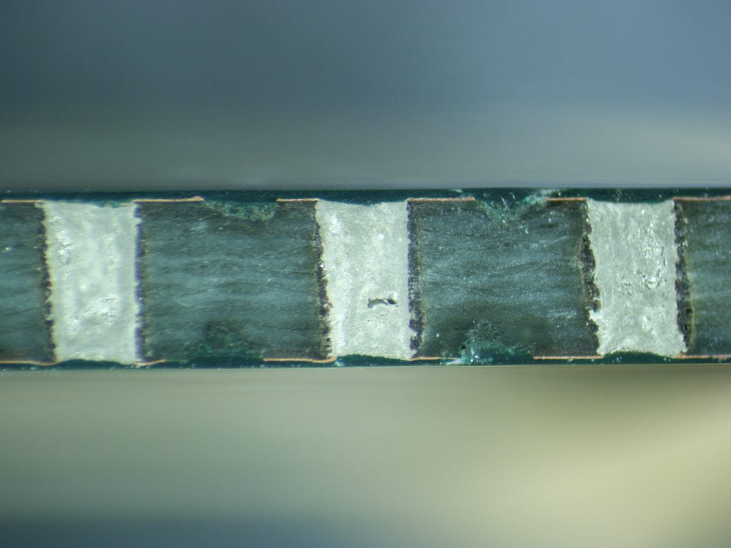
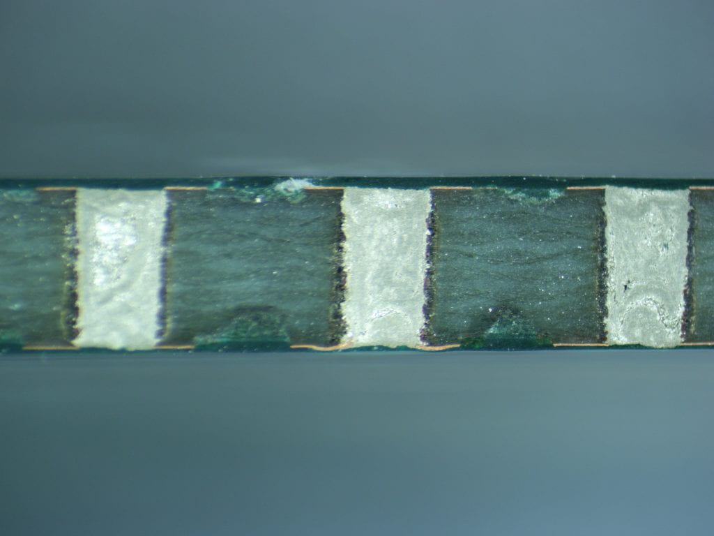
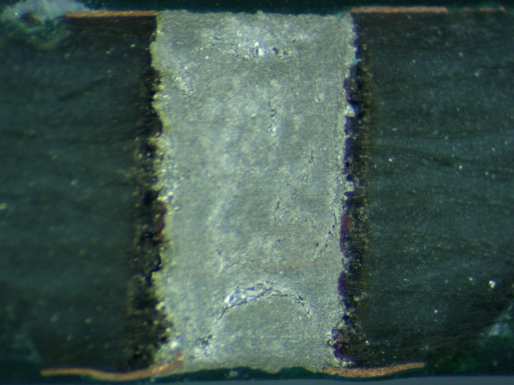
We roughly cut the PCB near the vias using circular cut-off wheel. The remainder of the PCB material was slowly removed using 800, 1500, and 3000 grit sand paper (wet sanding using the latter two). The PCBs were intermittently inspected during the wet sanding until all vias were exposed at their half-way mark. Images were captured using an 18MP camera on top of a Trinocular Stereo Zoom Microscope with a multizone circular LED (AmScope SM-4TZ-144A-18M3 3.5X-90X).
Scale can be inferred by via size (scale bar not included). Click between gallery images for near and far images of each via size.
0.2 / 0.4mm Via
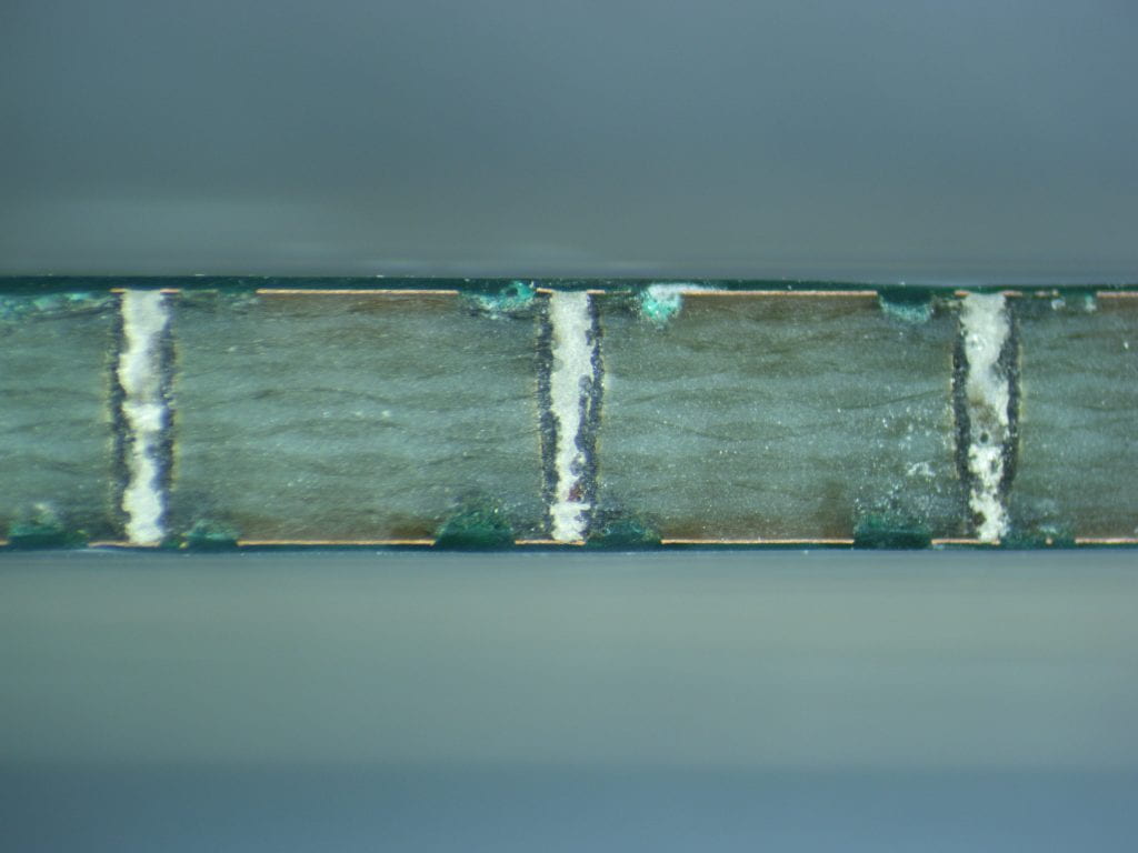
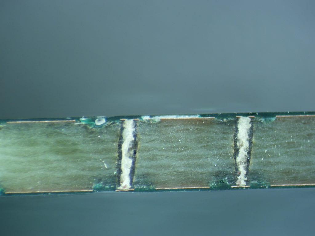
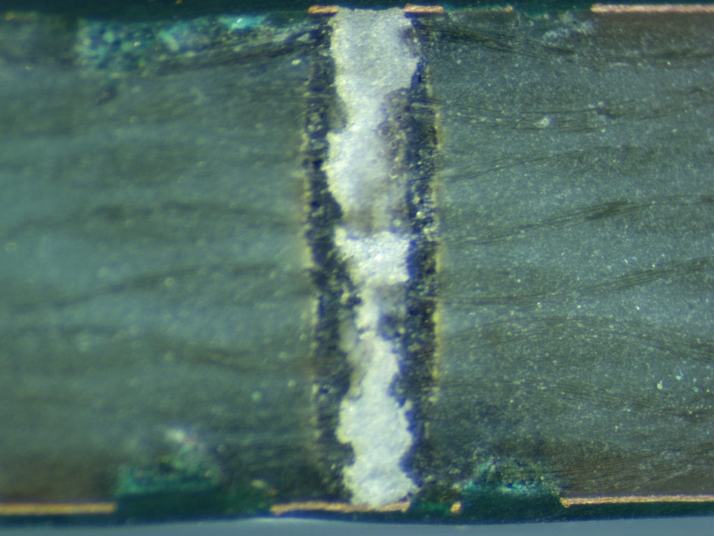
0.4 / 0.8mm Via
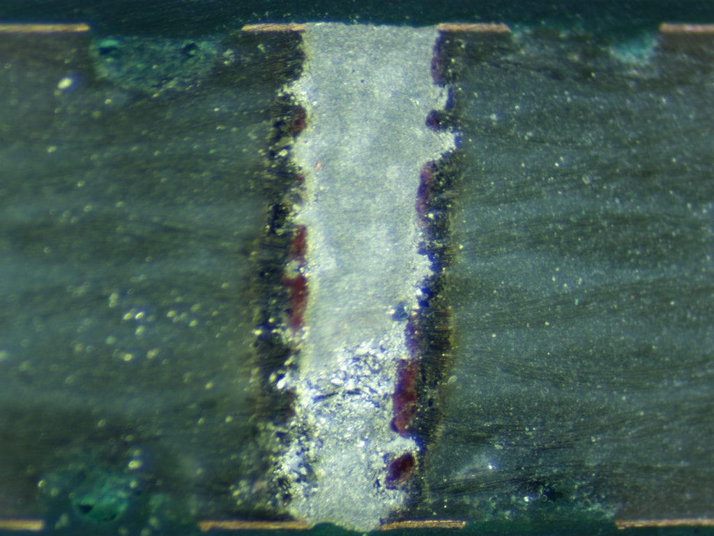
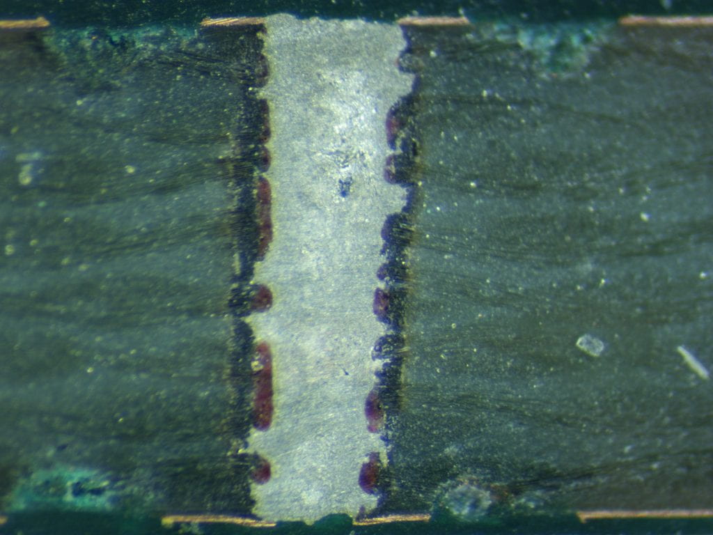
0.8 / 1.6mm Via
Functional Test
A multimeter (Fluke 106) with micro test leads was used to measure the resistance between both sides of the PCB (i.e., pad-to-pad) for the board that was not dissected. There were 6 vias total of each size oriented in linear triplets: this accounts for potential application inconsistencies across the length of the PCB.
| Sample | 0.2 / 0.4mm (Ω) | 0.4 / 0.8mm (Ω) | 0.9 / 1.6mm (Ω) |
|---|---|---|---|
| 1 | 1.2 | 0.8 | 2.7 |
| 2 | 1.3 | 0.9 | 4.4 |
| 3 | 2.2 | 1.7 | 0.5 |
| 4 | ∞ | 0.9 | 0.4 |
| 5 | 1 | 0.7 | 0.4 |
| 6 | 1.1 | 14,000 | 0.4 |
A few important observations:
- The 0.2/0.4mm sample #4 appeared to be an open circuit.
- The 0.4/0.8mm sample #6 had a very high resistance, suggesting a partial connection.
Discussion
It appears that 0.2/0.4mm vias are viable. It is unclear at the moment where issues emerge from, either the laser processing itself or the epoxy application. We anticipate several enhancements to protocol in the meantime:
- Cleaning PCBs at every stage to mitigate particulate contamination of the epoxy.
- Including a vacuum stage to assist in pulling epoxy through the vias.
As we grow into a new UV laser system with higher accuracy and refine our processes, we will keep this post updated with our results.